CETC, an active player in the Belt and Road (B&R) Initiative
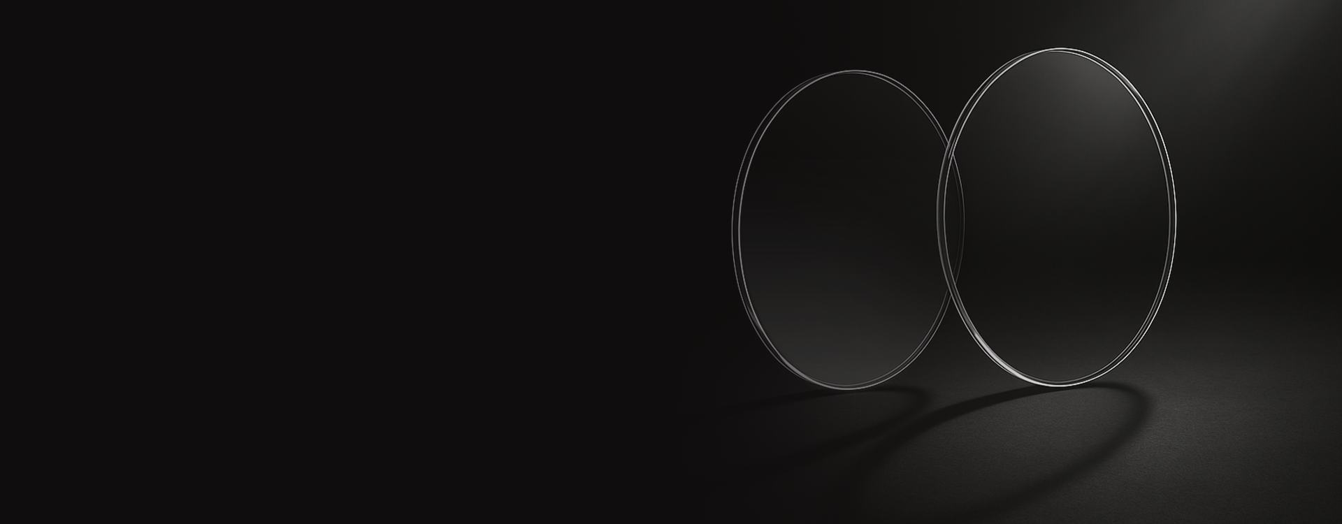
Diamond Substrate / Wafer
Diamond wafers represent a groundbreaking advancement in material science, offering properties far superior to conventional semiconductor materials like silicon. Unlike naturally occurring diamonds, these thin, precision-engineered slices are primarily manufactured through chemical vapor deposition (CVD), a process that allows for exceptional control over their purity, thickness, and crystal orientation. This synthesis method enables the creation of large-area, single-crystal diamond, overcoming the limitations of natural diamond's size and imperfections.
The appeal of diamond wafers lies in their extraordinary characteristics. Diamond boasts the highest known thermal conductivity, allowing for highly efficient heat dissipation, which is crucial for high-power electronic devices. It also exhibits an ultra-wide bandgap, leading to superior electrical insulation, high breakdown voltage, and minimal power loss, enabling devices to operate at higher voltages and temperatures. Furthermore, diamond is incredibly hard and chemically inert, offering exceptional durability and resistance to harsh environments. Its optical transparency across a broad spectrum, from UV to infrared, adds to its versatility.
These remarkable properties unlock a wide array of applications. In the electronics and semiconductor industry, diamond wafers serve as ideal substrates and heat spreaders for high-power devices such as transistors, diodes, and RF components, preventing overheating and enhancing performance. Their ability to handle extreme conditions makes them suitable for use in communications satellites and other aerospace applications. Beyond electronics, diamond wafers are finding applications in optics for high-performance windows and lenses, in medical devices due to their biocompatibility, and even in quantum computing for creating stable qubits. As manufacturing techniques continue to advance, diamond wafers are poised to revolutionize various high-tech sectors, pushing the boundaries of device performance and reliability.
CETC's diamond substrate is a high-quality large-diameter substrate in either single-crystal or polycrystalline form. It is made with original CVD method and wafer processing technology, which has been originally developed for many years. The features are exceptional thermal conductivity, high electron mobility, and high power capacity.
- Growth Method: Microwave Plasma Chemical Vapor Deposition (MPCVD) is the most common method for producing high-quality CVD diamond wafers.
- Material: Diamond (100% Carbon)
- Structure:
- Single-Crystal Diamond (SCD): Offers superior intrinsic properties due to its continuous crystal lattice. More challenging to grow in large sizes.
- Polycrystalline Diamond (PCD): Composed of multiple small, randomly oriented crystals. More readily available in larger sizes and generally lower cost than SCD. Properties like thermal conductivity can be slightly lower than SCD due to grain boundaries.
- Crystal Orientation (for SCD): Typically {100}, but {111} and other orientations may be available for specific applications.
- Density: Approximately 3.51 - 3.52 g/cm³
- Moh's Hardness: >10 (Diamond is the hardest known material)
- Young's Modulus: 1000 - 1100 GPa
- Tensile Strength: 450 - 1100 MPa (can vary with thickness)
- Poisson's Ratio: ~0.069 - 0.1
- Thermal Conductivity (T.C):
- Electronics/Thermal Management Grade: Highly critical parameter. Typically ranges from 1200 W/(m·K) to 2200 W/(m·K) at 300K, with higher values (e.g., >1800 W/(m·K)) being premium. Polycrystalline diamond might be in the 1000-2000 W/m.K range, while single-crystal can reach 2000-2200 W/m.K.
- Thermal Diffusivity (at 300K): Typically > 6.6 cm²/s (for 1200 W/m.K T.C) to > 10 cm²/s (for 2000 W/m.K T.C).
- Thermal Expansion Coefficient (RT-700℃): ~1.0 x 10⁻⁶ K⁻¹ to 3.1962 x 10⁻⁶ K⁻¹
- Bandgap: 5.47 eV (Ultra-wide bandgap)
- Dielectric Constant (at 1MHz): ~5.68 - 5.7
- Dielectric Loss (at 1MHz): Typically very low, e.g., 6.2 x 10⁻⁸
- Volume Resistivity (at 25℃): >10¹² to 10¹⁶ Ω·cm (highly insulating)
- Dielectric Strength/Insulation Withstand Voltage: >10 MV/cm (e.g., DC 5.5KV/1.5mA)
- Optical Transmittance: 40% - 70% (depending on grade and wavelength, e.g., >70% at 1064 nm for optical grade)
- Infrared Absorption Coefficient (e.g., @1.064um): 0.1871 - 0.3979 cm⁻¹
- Nitrogen Concentration (for SCD): Typically <0.5 ppm for high purity.
- Raman Full Width at Half Maximum (FWHM): ~2.1 cm⁻¹ (for SCD) for the diamond peak at 1332.5 cm⁻¹. Lower FWHM indicates higher crystal quality.
- Metallization: Customizable, e.g., Gold plating, Copper covering, AuSn solder. Patterning can also be customized.
- Doping (for electrical properties):
- p-type: Typically Boron doped.
- n-type: Typically Phosphorus, Antimony, or Arsenic doped (less common and more challenging).
- Packaging: Vacuum packaging, multi-piece packaging.
1-inch Diameter Diamond Wafer (approx. 25.4 mm)
- Diameter Tolerance: Typically +0.1 / -0 mm.
- Thickness: Highly customizable, ranging from 100 µm to 2 mm or more. Common thicknesses are 300 µm, 500 µm.
- Thickness Tolerance:
- For thickness ≤10 mm: ±0.02 mm
- For thickness 10-15 mm: ±0.03 mm
- Typical for ~300 µm: ±5%
- Surface Roughness (Ra):
- Front (Polished): Typically <1 nm, often specified as Ra < 1 nm. For coarse throw/lapping, Ra < 200 nm.
- Back: Typically <50 nm to <200 nm.
- Total Thickness Variation (TTV): Typically <1 µm (for Ø25mm).
- Bow: Typically <1 µm (for Ø25mm).
- Flatness PV (Peak-to-Valley, e.g., @633nm): <1.5 fringe (for Ø25mm).
- Warp: Not always explicitly stated for 1-inch, but generally very low due to strict TTV/Bow specs.
2-inch Diameter Diamond Wafer (approx. 50.8 mm)
- Diameter Tolerance: Typically +0.1 / -0 mm.
- Thickness: Customizable, similar range to 1-inch wafers (e.g., 100 µm to 2 mm). Common thicknesses are 0.3 mm (300 µm) or 0.5 mm (500 µm).
- Thickness Tolerance: Typically ±5% for 0.3mm thickness.
- Surface Roughness (Ra):
- Front (Polished): Typically <1 nm.
- Back: Typically <50 nm.
- Total Thickness Variation (TTV): Typically <60 µm. Values as low as <10 µm can be found for premium wafers.
- Bow: Typically <200 µm. Values as low as <50 µm or <30 µm can be found.
- Warp: Typically <50 µm.
- FWHM (XRC 004 for heteroepitaxial growth on sapphire): As low as 98 arcsec for high crystal quality.